Chapterبەش 10 · Lectureوانە 10.2
Latches and Flip-Flops: One Bit of Memoryلاچەکان و فلیپ-فلۆپەکان: بیرگەی یەک بیتی
How a circuit remembers: feedback, the SR latch (NOR and NAND), the gated D latch, level and edge triggering, the edge-triggered D flip-flop (master–slave), JK and T flip-flops, characteristic tables and equations, preset and clear, and timing diagrams read edge by edge.
چۆن لەبیری دەمێنێت: ، SR (NOR و NAND)، Dـی دەرگادار، چالاکبوون بە ئاست و بە لێوار، Dـی لێوار-چالاک (سەرەکی و پاشکۆ)، JK و T، و ، preset و clear و خوێندنەوەی لێوار بە لێوار.
What you will learnچی فێر دەبیت
- Explain how feedback turns gates into a one-bit memory, and trace the SR latch (NOR and NAND).
- Tell a level-triggered latch from an edge-triggered flip-flop in a timing diagram.
- Use the characteristic tables and equations of SR, D, JK and T flip-flops.
- Explain preset and clear, and complete timing diagrams edge by edge.
- ڕوون بکەیتەوە چۆن دەکات بە یەک و SR (NOR و NAND) هەنگاو بە هەنگاو بپشکنیت.
- لە ئاست-چالاک لە لێوار-چالاک جیا بکەیتەوە.
- و SR، D، JK و T بەکار بهێنیت.
- preset و clear ڕوون بکەیتەوە و لێوار بە لێوار تەواو بکەیت.
Circuits that rememberسووڕەکانی خاوەن بیرگە
Every circuit in the course so far — gates, adders, multiplexers, decoders — is combinational: its output depends only on the inputs at this moment. Change the inputs back and the output forgets everything. A computer also needs circuits that remember: the number you just typed, the next instruction, a running count. Their output depends on the present inputs and on what happened before. These are sequential circuits (What comes next introduced the idea).
هەموو کۆرسەکە تا ئێستا — ، ، ، — تێکەڵەییـە: تەنها بەندە بە ئەم ساتە. بگەڕێنەرەوە و هەموو شتێک لەبیر دەکات. پێویستی بە وەهاش هەیە کە لەبیریان بمێنێت: ئەو ژمارەیەی ئێستا نووسیت، داهاتوو، ژمارەیەک کە دەژمێردرێت. ئەمانە بەندە بە ئێستا و بەوەی پێشتر ڕوویداوە. ئەمانە ن (دواتر چی دێت بیرۆکەکەی ناساند).
| Combinationalتێکەڵەیی | Sequentialزنجیرەیی | |
|---|---|---|
| Output depends on بەندە بە | the present inputs onlyتەنها ئێستا | the present inputs and the stored state ئێستا و دۆخی هەڵگیراو |
| Memory | noneنییە | latches and flip-flops و |
| Examplesنموونە | adder, multiplexer, decoder، ، | register, counter, the CPU، ، |
Circuits that rememberسووڕەکانی خاوەن بیرگە
What a one-bit memory needsبیرگەی یەک بیت پێویستی بە چییە
Press the call button of a lift and take your finger away: the button stays lit until the lift arrives. The light depends not on what your finger is doing now, but on something that happened earlier. A doorbell button is the opposite: it rings only while you press — a combinational circuit.
دوگمەی بانگکردنی ئاسانسۆرێک دابگرە و پەنجەت لابەرە: دوگمەکە ڕووناک دەمێنێتەوە تا ئاسانسۆرەکە دەگات. ڕووناکییەکە بەند نییە بەوەی ئێستا پەنجەت چی دەکات، بەڵکو بە شتێک کە پێشتر ڕوویداوە. دوگمەی زەنگی دەرگا پێچەوانەکەیە: تەنها کاتێک زەنگ لێدەدات کە دایدەگریت — .
Where the analogy stops workingسنووری ئەم نموونەیە
The lift button is a whole small system; inside it, a one-bit memory like the latches of this lesson keeps the light on.
دوگمەی ئاسانسۆر سیستەمێکی بچووکی تەواوە؛ لەناویدا یەک وەک ئەم وانەیە چراکە بە هەڵکراوی دەهێڵێتەوە.
A device that stores a bit needs three things: two stable states (one for 0, one for 1), a way to read the state, and a way to set it. The circuits of this lesson build all three from ordinary gates.
ئامێرێک کە هەڵدەگرێت پێویستی بە سێ شتە: دوو دۆخی جێگیر (یەکێک بۆ 0 و یەکێک بۆ 1)، ڕێگایەک بۆ خوێندنەوەی دۆخەکە و ڕێگایەک بۆ دانانی. ئەم وانەیە هەر سێکیان لە ئاسایی دروست دەکەن.
Circuits that rememberسووڕەکانی خاوەن بیرگە
Feedback: a loop in the circuitفیدباک: بازنەیەک لەناو سووڕدا
Connecting a circuit's output back to one of its own inputs. Feedback gives a circuit memory (a keeps its state) or, with an odd number of inverters in the loop, makes it oscillate.
بەستنەوەی سووڕێک بە یەکێک لە خودی خۆی. فیدباک دەدات بە سووڕەکە ( دۆخەکەی دەپارێزێت)، یان ئەگەر ژمارەیەکی تاک لە بازنەکەدا بێت، وای لێ دەکات بلەرێتەوە.
Every circuit so far sends signals one way, from inputs to outputs. To remember, a circuit needs feedback: an output wired back to an input. The simplest case is two NOT gates in a loop. If the first outputs 0, the second outputs 1, which keeps the first at 0 — the loop holds itself in that state forever. The opposite state (1 and 0) is just as stable. A circuit with two stable states is called bistable, and that is exactly one bit of memory.
هەموو تا ئێستا بە یەک ئاڕاستە دەنێرێت، لە بۆ . بۆ ئەوەی لەبیری بمێنێت، پێویستی بە هەیە: کە بگەڕێنرێتەوە بۆ . سادەترین نموونە دوو لە بازنەیەکدا. ئەگەر یەکەمیان 0 بدات، دووەمیان 1 دەدات کە یەکەمیان لە 0دا دەهێڵێتەوە — بازنەکە خۆی بۆ هەمیشە لەو دۆخەدا ڕادەگرێت. دۆخە پێچەوانەکەش (1 و 0) هەر ئەوەندە جێگیرە. کە دوو دۆخی جێگیری هەبێت پێی دەوترێت دوو-جێگیر (bistable) و ئەمە ڕێک یەک .
Feedback can also do the opposite. Put an odd number of NOT gates in a ring — three, say — and no state is stable: each gate keeps flipping the next one, so the output oscillates. Such a ring oscillator is a simple clock source; its speed depends on the gate delays.
دەتوانێت پێچەوانەکەش بکات. ژمارەیەکی تاک — بۆ نموونە سێ — لە ئەڵقەیەکدا دابنێ و هیچ دۆخێک جێگیر نابێت: هەر بەردەوام دواترین هەڵدەگەڕێنێتەوە، بۆیە دەلەرێتەوە. ئەم لەرەرە ئەڵقەییە (ring oscillator) سەرچاوەیەکی سادەی ؛ خێراییەکەی بەندە بە دواکەوتنی .
The SR latch: set, reset, holdلاچی SR: دانان، سفرکردنەوە، ڕاگرتن
A simple memory circuit that stores one bit and keeps it until its inputs change it. A latch is built from gates connected in a loop (feedback).
سووڕێکی بیرگەی سادەیە کە یەک هەڵدەگرێت و دەیپارێزێت تا دەیگۆڕن. لە چەند دروست دەکرێت کە لە بازنەیەکدا بەیەکەوە بەستراون (فیدباک).
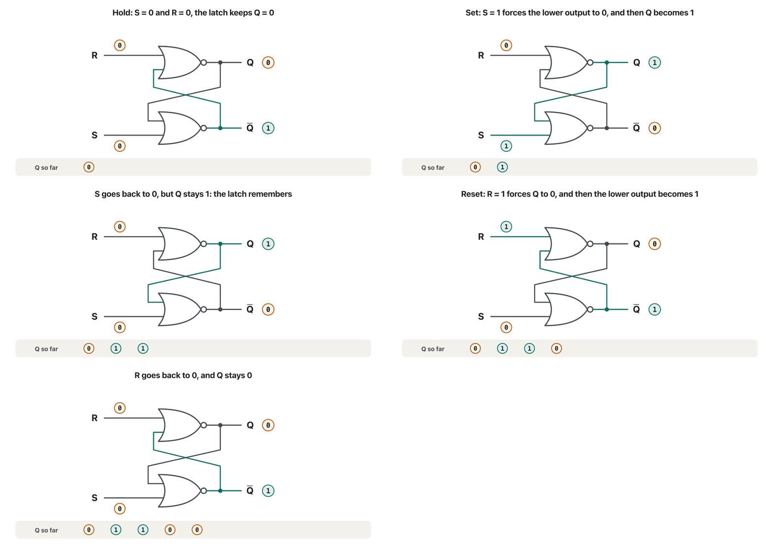
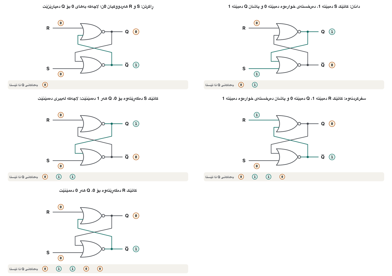
Replace the two NOT gates of the loop by two NOR gates. Each gate keeps one input for the feedback and gets one free input: S (set) and R (reset). The outputs are Q and its complement . With a NOR gate acts like a NOT gate, so the loop simply holds its state. Watch what a short 1 on S, and later on R, does:
لە جیاتی دوو بازنەکە، دوو دابنێ. هەر یەک بۆ دەهێڵێتەوە و یەک ئازاد وەردەگرێت: S (set، دانان) و R (reset، سفرکردنەوە). Q و ، ـن. کاتێک بێت، وەک کار دەکات، بۆیە بازنەکە تەنها دۆخەکەی خۆی ڕادەگرێت. سەیر بکە 1ـێکی کورت لەسەر S و دواتر لەسەر R چی دەکات:
| S R | Q (next)Q (داهاتوو) | Actionکار |
|---|---|---|
| 0 0 | Q | hold: keep the stored bitڕاگرتن: هەڵگیراوەکە دەپارێزێت |
| 0 1 | 0 | resetسفرکردنەوە |
| 1 0 | 1 | setدانان |
| 1 1 | – | not allowedڕێگەپێنەدراو |
Why does it work? A NOR gate outputs 0 as soon as any input is 1. So forces to 0; the top gate then sees and and outputs . When S drops back to 0, the bottom gate still sees on its other input, so stays 0 and Q stays 1.
بۆچی کار دەکات؟ هەر کە هەر 1 بێت 0 دەدات. بۆیە دەکاتە 0؛ پاشان سەرەوە و دەبینێت و دەدات. کاتێک S دەگەڕێتەوە بۆ 0، خوارەوە هێشتا لەسەر تری دەبینێت، بۆیە هەر 0 و Q هەر 1 دەمێنێت.
Builds a latch from NOR gates on a breadboard and shows how feedback lets it set, reset and remember one bit.
لە لەسەر دروست دەکات و پیشان دەدات چۆن ڕێگە دەدات دابنرێت، سفر بکرێتەوە و یەک لەبیر بهێڵێتەوە.
Ben Eater: the SR latch built and tested on a breadboard (9:30 the SR latch).
Ben Eater: SR لەسەر دروست دەکرێت و تاقی دەکرێتەوە (9:30 SR).
The SR latch: set, reset, holdلاچی SR: دانان، سفرکردنەوە، ڕاگرتن
and : the forbidden input و : نێوخستە قەدەغەکراوەکە
What if S and R are both 1? Each NOR gate has a 1 on an input, so both outputs become 0. Now Q and are equal, which breaks the rule that is the complement of Q. Worse, when S and R return to 0 at the same moment, both gates try to switch to 1 together: the latch may end up in either state, or even oscillate for a while. This is a race, and nobody can say the result in advance.
ئەگەر S و R هەردووکیان 1 بن چی دەبێت؟ هەر 1ـێکی لەسەر هەیە، بۆیە هەردوو دەبنە 0. ئێستا Q و یەکسانن کە ئەو یاسایە دەشکێنێت کە Qـیە. خراپتر ئەوەیە کاتێک S و R لە هەمان ساتدا دەگەڕێنەوە بۆ 0، هەردوو پێکەوە هەوڵ دەدەن ببنە 1: لەوانەیە بگاتە هەر یەکێک لە دوو دۆخەکە، یان تەنانەت ماوەیەک بلەرێتەوە. ئەمە پێشبڕکێیە (race) و کەس ناتوانێت پێشوەختە ئەنجامەکە بڵێت.
So the rule for the SR latch is: never make S and R 1 together, written . Under that rule its behaviour is described by one equation, where is the next value of Q:
بۆیە یاسای SR ئەمەیە: هەرگیز S و R پێکەوە مەکە بە 1، کە دەنووسرێت . بەپێی ئەو یاسایە ڕەفتارەکەی بە یەک وەسف دەکرێت، کە بەهای داهاتووی Qـیە:
Read it as: the next Q is 1 if S sets it, or if it was already 1 and R does not reset it.
بیخوێنەوە: Qـی داهاتوو 1ـە ئەگەر S دایبنێت، یان ئەگەر پێشتر 1 بووبێت و R سفری نەکاتەوە.
The SR latch: set, reset, holdلاچی SR: دانان، سفرکردنەوە، ڕاگرتن
The NAND latch: active-low inputsلاچی NAND: نێوخستەکانی چالاک بە LOW
The same latch can be built from two cross-coupled NAND gates. A NAND gate is forced by a 0 on an input, so here the inputs are active-low: they rest at 1, and a short 0 on sets the latch, a short 0 on resets it. The bars in the names remind you of this.
هەمان دەتوانرێت لە دوو بەیەکەوەبەستراو دروست بکرێت. بە 0ـێک لەسەر ناچار دەکرێت، بۆیە لێرەدا چالاکن بە LOW: لە دۆخی ئاساییدا 1ـن و 0ـێکی کورت لەسەر دادەنێت، 0ـێکی کورت لەسەر سفری دەکاتەوە. هێڵی سەر ناوەکان ئەمەت بیر دەخاتەوە.
| S̄ R̄ | Q (next)Q (داهاتوو) | Actionکار |
|---|---|---|
| 1 1 | Q | holdڕاگرتن |
| 0 1 | 1 | setدانان |
| 1 0 | 0 | resetسفرکردنەوە |
| 0 0 | – | not allowed (both outputs 1)ڕێگەپێنەدراو (هەردوو 1ـن) |
A real use: a mechanical switch bounces — its contacts hit and spring apart several times in a few milliseconds, so a counter would see many presses. Wire a changeover switch to the and inputs of a NAND latch: the first touch sets or resets the latch, and the bounces cannot change it back. The 74HC279 chip holds four such latches.
بەکارهێنانێکی ڕاستەقینە: میکانیکی دەلەرێتەوە (bounce) — خاڵەکانی لە چەند میلی چرکەیەکدا چەند جار بەر یەک دەکەون و جیا دەبنەوە، بۆیە چەندین داگرتن دەبینێت. دوو-ڕێ بە و ـی NAND ببەستە: یەکەم بەرکەوتن دادەنێت یان سفری دەکاتەوە و لەرینەوەکان ناتوانن بیگەڕێننەوە. 74HC279 چوار وەهای تێدایە.
The gated latch and the D latchلاچی دەرگادار و لاچی D
An SR latch reacts at once to S and R. Usually we want to decide when it may change. Add two AND gates in front of S and R, both controlled by an enable input EN (also called C or G): when both AND outputs are 0, so the latch holds; when , S and R pass through. This is a gated SR latch.
SR دەستبەجێ وەڵامی S و R دەداتەوە. زۆرجار دەمانەوێت بڕیار بدەین کەی دەتوانێت بگۆڕێت. دوو لە پێش S و R دابنێ کە هەردووکیان بە چالاککردن، EN (یان C یان G)، کۆنترۆڵ دەکرێن: کاتێک بێت، هەردوو ANDـەکە 0ـە، بۆیە ڕادەگرێت؛ کاتێک بێت، S و R تێدەپەڕن. ئەمە SRـی دەرگادارە.
One more step removes the forbidden input. Give the latch a single data input D, send D to S and its complement to R. Now S and R are always opposite, so they can never both be 1. This is the D latch (D for data):
هەنگاوێکی تر قەدەغەکراوەکە لادەبات. تەنها یەک ، D، بدە بە ، D بنێرە بۆ S و ، ، بۆ R. ئێستا S و R هەمیشە پێچەوانەی یەکن، بۆیە هەرگیز ناتوانن پێکەوە 1 بن. ئەمە Dـیە (D بۆ data):
Adds an enable input to the SR latch and turns it into a D latch that stores one bit while enabled.
چالاککردن بۆ SR زیاد دەکات و دەیکاتە D، کە لە کاتی چالاکبووندا یەک هەڵدەگرێت.
Ben Eater: 2:51 adding an enable to the SR latch, 8:08 the D latch.
Ben Eater: 2:51 زیادکردنی چالاککردن بۆ SR، 8:08 D.
The gated latch and the D latchلاچی دەرگادار و لاچی D
Transparent while enabledڕوون لە کاتی چالاکبووندا
| EN | D | Q (next)Q (داهاتوو) |
|---|---|---|
| 0 | X | Q (hold)Q (ڕاگرتن) |
| 1 | 0 | 0 |
| 1 | 1 | 1 |
While the D latch is transparent: Q simply follows D, like looking through a window. When EN goes to 0 the window closes and Q keeps the last value D had. Chips such as the 74HC75 (4 bits) and the 74HC573 (8 bits) are rows of D latches, used to hold a value from a bus.
لە کاتی ، D ڕوونە (transparent): Q تەنها دوای D دەکەوێت، وەک سەیرکردن بە پەنجەرەدا. کاتێک EN دەبێتە 0، پەنجەرەکە دادەخرێت و Q دوایین بەهای Dـی پێوە دەمێنێت. وەک 74HC75 (4 ) و 74HC573 (8 ) ڕیزێک لە Dـن کە بۆ هەڵگرتنی بەهایەک لە بەکار دێن.
The clock: level or edge?سیگناڵی کاتژمێر: ئاست یان لێوار؟
Real systems use a clock: a square wave that ticks at a steady rate (pulses, period and frequency). Put the clock on EN and every latch may change only while the clock is HIGH. That is level triggering. It has a weakness: during the whole HIGH half of a period the latch is transparent, so if its output feeds back, through other gates, into its own input, a new value can race round the loop several times in one tick.
سیستەمە ڕاستەقینەکان بەکار دەهێنن: کە بە ڕێژەیەکی جێگیر لێدەدات (تڕپەکان، کاتی خولی و لەرەلەر). بدە بە EN و هەموو تەنها لە کاتی HIGH بوونی دەتوانێت بگۆڕێت. ئەمە چالاکبوون بە ئاستە (level triggering). کەموکوڕییەکی هەیە: لە هەموو نیوەی HIGHـی ڕوونە، بۆیە ئەگەر بە تردا بگەڕێتەوە بۆ خۆی، بەهایەکی نوێ دەتوانێت لە یەک لێداندا چەند جار بە بازنەکەدا بخولێتەوە.
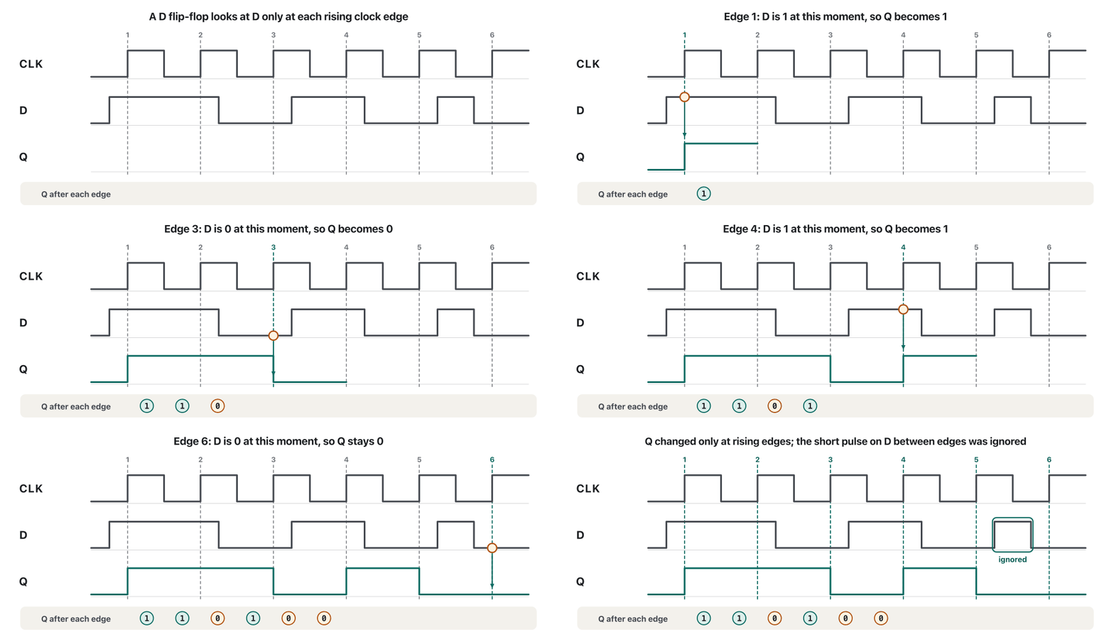
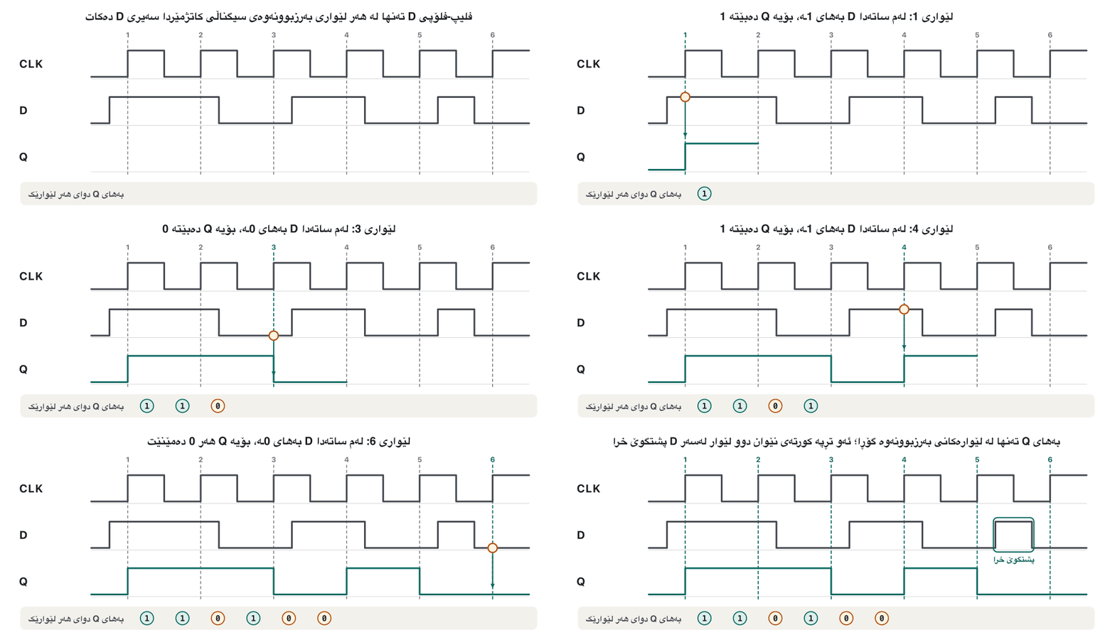
The cure is edge triggering: the circuit samples its input only at the instant the clock changes, usually at the rising edge (0 → 1), and ignores the input the rest of the time. Such a circuit is a flip-flop. Every flip-flop in a system changes at the same instant, once per clock period — this is what keeps a whole processor in step. A timing diagram shows the difference best:
چارەسەرەکە چالاکبوون بە لێوارە (edge triggering): تەنها لەو ساتەدا دەخوێنێتەوە کە دەگۆڕێت، زۆرجار لە (0 بۆ 1) و لە هەموو کاتەکانی تردا پشتگوێ دەخات. وەها . هەموو لە سیستەمێکدا لە هەمان ساتدا دەگۆڕێت، لە هەر یەک جار — ئەمەیە کە پرۆسێسەرێکی تەواو هاوهەنگاو دەهێڵێتەوە. هێڵکاریی کاتبەندی باشترین شێوە جیاوازییەکە پیشان دەدات:
The clock: level or edge?سیگناڵی کاتژمێر: ئاست یان لێوار؟
Latch or flip-flop?لاچ یان فلیپ-فلۆپ؟
A latch is like a phone camera filming while you hold the button: everything that happens in that time is recorded. A flip-flop is like taking one photo at the click: only that instant counts.
وەک کامێرای مۆبایلێکە کە تا دوگمەکە دابگریت ڤیدیۆ دەگرێت: هەموو ئەوەی لەو ماوەیەدا ڕوو دەدات تۆمار دەکرێت. وەک گرتنی یەک وێنەیە لە ساتی کلیککردندا: تەنها ئەو ساتە گرنگە.
Where the analogy stops workingسنووری ئەم نموونەیە
A real edge is not perfectly instant: the input must be steady for a tiny time before and after it (the setup and hold times).
لێوارێکی ڕاستەقینە تەواو دەستبەجێ نییە: دەبێت بۆ کاتێکی زۆر کەم پێش و دوای ئەو جێگیر بێت (کاتەکانی setup و hold).
The D flip-flopفلیپ-فلۆپی D
A one-bit memory circuit that changes only at the edge of a clock pulse. Flip-flops are the building blocks of registers and counters.
سووڕێکی بیرگەی یەک بیتییە کە تەنها لە لێواری دەگۆڕێت. فلیپ-فلۆپەکان بەردی بناغەی و .
The D flip-flop is the workhorse of digital design. At each rising edge of CLK it copies D to Q; between edges Q does not change, whatever D does. In one line: , sampled at the edge. On the symbol, the small triangle at the clock input means "edge-triggered". Follow it edge by edge:
D بەکارهاتووترین بلۆکی دیزاینی . لە هەر CLKـدا D کۆپی دەکات بۆ Q؛ لە نێوان لێوارەکاندا Q ناگۆڕێت، D هەرچی بکات. بە یەک دێڕ: ، کە لە لێوارەکەدا دەخوێنرێتەوە. لەسەر ، سێگۆشە بچووکەکەی سەر واتە «لێوار-چالاک». لێوار بە لێوار بەدوایدا بڕۆ:
A D flip-flop is the natural way to store one bit at a chosen moment, and it is the cell of registers and shift registers in the next lesson. The 74HC74 chip has two D flip-flops, each with preset and clear inputs (see below).
D ڕێگای سروشتیی هەڵگرتنی یەک لە ساتێکی هەڵبژێردراودا و خانەی و جووڵاندنە لە وانەی داهاتوو. 74HC74 دوو Dـی هەیە کە هەر یەکەیان preset و clearـی هەیە (لە خوارەوە بڕوانە).
Latch versus edge-triggered D flip-flop on a timing diagram: Q copies D only at the rising edge of the clock.
بەرامبەر Dـی لێوار-چالاک لەسەر : Q تەنها لە D کۆپی دەکات.
Plays 0:00–5:47: the timing diagram, latch versus flip-flop, and how a D flip-flop copies D only at the rising clock edge.
لە 0:00 تا 5:47 پەخش دەبێت: ، بەرامبەر و D چۆن تەنها لە D کۆپی دەکات.
The D flip-flopفلیپ-فلۆپی D
Inside an edge-triggered flip-flop: master and slaveناوەوەی فلیپ-فلۆپێکی لێوار-چالاک: سەرەکی و پاشکۆ
How can gates react to an edge? One classic way chains two D latches, the master and the slave, with opposite enables. While the master is open and follows D, and the slave is closed, so Q does not move. At the rising edge the master closes and keeps the last D, and at the same moment the slave opens and passes that value to Q. While the slave is open but the master is closed, so changes on D cannot get through. Q can therefore change only at the rising edge.
چۆن دەتوانن وەڵامی لێوارێک بدەنەوە؟ ڕێگایەکی کلاسیکی دوو D، سەرەکی (master) و پاشکۆ (slave)، بە چالاککردنی پێچەوانە بە زنجیر دەبەستێت. لە کاتی سەرەکییەکە کراوەیە و دوای D دەکەوێت و پاشکۆکە داخراوە، بۆیە Q ناجووڵێت. لە سەرەکییەکە دادەخرێت و دوایین D ڕادەگرێت و لە هەمان ساتدا پاشکۆکە دەکرێتەوە و ئەو بەهایە دەگەیەنێتە Q. لە کاتی پاشکۆکە کراوەیە بەڵام سەرەکییەکە داخراوە، بۆیە گۆڕانەکانی D ناتوانن تێپەڕن. کەواتە Q تەنها لە دەتوانێت بگۆڕێت.
Real chips often use a cleverer circuit of three small latches (and old master–slave JK chips such as the 7476 change their outputs at the falling edge), but from the outside every edge-triggered flip-flop behaves the same: one sample per active edge.
ڕاستەقینەکان زۆرجار زیرەکتر لە سێ بچووک بەکار دەهێنن (و JKـی سەرەکی-پاشکۆی کۆنی وەک 7476 لە دەگۆڕن)، بەڵام لە دەرەوە هەموو لێوار-چالاک هەمان ڕەفتاری هەیە: بۆ هەر لێوارێکی چالاک یەک خوێندنەوە.
The JK flip-flop: set, reset, hold or toggleفلیپ-فلۆپی JK: دانان، سفرکردنەوە، ڕاگرتن یان هەڵگەڕانەوە
The JK flip-flop is an edge-triggered SR flip-flop that turns the forbidden input into something useful. J works like S (set) and K like R (reset); with the flip-flop toggles — Q changes to its opposite at the edge.
JK SRـی لێوار-چالاکە کە قەدەغەکراوەکە دەکات بە شتێکی بەسوود. J وەک S کار دەکات (دانان) و K وەک R (سفرکردنەوە)؛ کاتێک بێت، هەڵدەگەڕێتەوە (toggle) — Q لە لێوارەکەدا دەبێتە پێچەوانەی خۆی.
| J K | Q⁺ (after the edge)Q⁺ (دوای لێوار) | Actionکار |
|---|---|---|
| 0 0 | Q | holdڕاگرتن |
| 0 1 | 0 | resetسفرکردنەوە |
| 1 0 | 1 | setدانان |
| 1 1 | toggleهەڵگەڕانەوە |
If Q is 0, the next Q is J (only J can set it). If Q is 1, the next Q is NOT K (only K can reset it).
ئەگەر Q 0 بێت، Qـی داهاتوو Jـە (تەنها J دەتوانێت دایبنێت). ئەگەر Q 1 بێت، Qـی داهاتوو NOT Kـە (تەنها K دەتوانێت سفری بکاتەوە).
The JK flip-flop can imitate the others: with it is a D flip-flop, and with J and K joined it is a T flip-flop. The 7476 chip of the counter lab in the next lesson holds two JK flip-flops with preset and clear; it changes on the falling edge, which its symbol shows with a bubble before the triangle.
JK دەتوانێت لاسایی ئەوانی تر بکاتەوە: بە دەبێتە D و بە بەستنەوەی J و K بە یەکەوە دەبێتە T. 7476 کە لە تاقیگەی وانەی داهاتوو بەکار دێت دوو JKـی هەیە بە preset و clear؛ لە دەگۆڕێت، کە بە بازنەیەک لە پێش سێگۆشەکە پیشانی دەدات.
The T flip-flop: toggle and divide by twoفلیپ-فلۆپی T: هەڵگەڕانەوە و دابەشکردن بەسەر دوودا
The T flip-flop (T for toggle) has one input. holds, toggles at every active edge. It is a JK flip-flop with J and K tied together, or a D flip-flop with :
T (T بۆ toggle، هەڵگەڕانەوە) یەک هەیە. ڕادەگرێت، لە هەر لێوارێکی چالاکدا هەڵدەگەڕێتەوە. ئەمە JKـیە کە J و K بە یەکەوە بەستراون، یان Dـیە بە :
Hold T at 1 and Q changes once per clock period, so a whole period of Q takes two clock periods: the flip-flop divides the frequency by 2. A 1 kHz clock gives 500 Hz at Q. Chain three of them and you divide by : 8 MHz becomes 1 MHz. A quartz watch counts the 32,768 Hz of its crystal down to exactly 1 Hz with 15 such stages, because . Chains like this are the counters of the next lesson.
T لە 1دا ڕابگرە و Q لە هەر یەک جار دەگۆڕێت، بۆیە تەواوی Q دوو دەخایەنێت: دابەش دەکات بەسەر 2دا. 1 kHz لە Q 500 Hz دەدات. سێیان بە زنجیر ببەستە و بەسەر دا دابەشی دەکەیت: 8 MHz دەبێتە 1 MHz. کاتژمێرێکی کوارتز 32,768 Hzـی کریستاڵەکەی بە 15 قۆناغی وەها دەژمێرێت تا دەگاتە ڕێک 1 Hz، چونکە . زنجیری وەها وانەی داهاتوون.
The four types side by sideچوار جۆرەکە لە تەنیشت یەک
Each flip-flop type is described by a characteristic table — the next state (after the edge) for every input and present state Q — or by the matching characteristic equation. Q is the bit stored now; is the bit stored after the next active edge.
هەر جۆرێکی بە وەسف دەکرێت — دۆخی داهاتوو (دوای لێوار) بۆ هەر و دۆخی ئێستای Q — یان بە ـی هاوتای. Q ئەو کە ئێستا هەڵگیراوە؛ ئەو کە دوای لێواری چالاکی داهاتوو هەڵدەگیرێت.
| Typeجۆر | Inputs → Q⁺ ← Q⁺ | Characteristic equation |
|---|---|---|
| SR | 00 hold, 01 → 0, 10 → 1, 11 not allowed00 ڕاگرتن، 01 ← 0، 10 ← 1، 11 ڕێگەپێنەدراو | |
| JK | 00 hold, 01 → 0, 10 → 1, 11 toggle00 ڕاگرتن، 01 ← 0، 10 ← 1، 11 هەڵگەڕانەوە | |
| D | 0 → 0, 1 → 10 ← 0، 1 ← 1 | |
| T | 0 hold, 1 toggle0 ڕاگرتن، 1 هەڵگەڕانەوە |
Every equation comes from an ordinary truth table with Q as one more input. For the JK flip-flop, with all eight rows:
هەموو لە ئاسایی دێت کە Q زیادەیە تێیدا. بۆ JK، بە هەر هەشت ڕیزەکەوە:
| J K Q | Q⁺ |
|---|---|
| 0 0 0 | 0 |
| 0 0 1 | 1 |
| 0 1 0 | 0 |
| 0 1 1 | 0 |
| 1 0 0 | 1 |
| 1 0 1 | 1 |
| 1 1 0 | 1 |
| 1 1 1 | 0 |
in rows 001, 100, 101 and 110. Grouping them on a Karnaugh map gives (rows 100, 110) and (rows 001, 101): exactly the equation above.
لە ڕیزەکانی 001، 100، 101 و 110دا. گرووپکردنیان لەسەر نەخشەیەکی کارنۆ (ڕیزەکانی 100، 110) و (ڕیزەکانی 001، 101) دەدات: ڕێک سەرەوە.
Preset and clear: acting without the clockPreset و clear: کارکردن بێ سیگناڵی کاتژمێر
When the power comes on, every flip-flop wakes up in a random state. So most flip-flop chips have two extra direct (asynchronous) inputs: preset forces and clear forces , at once, without waiting for a clock edge. On chips such as the 74HC74 and the 7476 they are active-low, written and . A reset button that clears every flip-flop of a circuit uses them.
کاتێک کارەبا دێت، هەموو بە دۆخێکی هەڕەمەکی هەڵدەستێت. بۆیە زۆربەی دوو زیادەی ڕاستەوخۆیان (ناهاوکات) هەیە: preset دەسەپێنێت و clear دەسەپێنێت، دەستبەجێ، بێ چاوەڕوانیی لێوارێکی . لە وەک 74HC74 و 7476دا چالاکن بە LOW و بەم شێوەیە دەنووسرێن: و . دوگمەیەکی reset کە هەموو سفر دەکاتەوە ئەمانە بەکار دەهێنێت.
| PRE̅ | CLR̅ | Q |
|---|---|---|
| 1 | 1 | normal: changes only at clock edgesئاسایی: تەنها لە لێوارەکانی دەگۆڕێت |
| 0 | 1 | 1 at once1، دەستبەجێ |
| 1 | 0 | 0 at once0، دەستبەجێ |
| 0 | 0 | not allowedڕێگەپێنەدراو |
Reading timing diagrams step by stepخوێندنەوەی هێڵکارییەکانی کاتبەندی هەنگاو بە هەنگاو
Exam questions often give the clock and the inputs and ask for Q. Use the same four steps for every flip-flop:
پرسیارەکانی تاقیکردنەوە زۆرجار و دەدەن و Q دەپرسن. بۆ هەموو هەمان چوار هەنگاو بەکار بهێنە:
Mark every active edge with a vertical line (rising edges, unless the symbol shows a bubble).
هەموو لێوارێکی چالاک بە هێڵێکی ستوونی دیاری بکە (، مەگەر بازنەیەک پیشان بدات).
At each edge, read the inputs just before the edge.
لە هەر لێوارێکدا ڕێک پێش لێوارەکە بخوێنەوە.
Apply the characteristic table to get from the inputs and the present Q.
جێبەجێ بکە بۆ وەرگرتنی لە و Qـی ئێستا.
Draw Q flat until the next edge — whatever the inputs do in between.
Q ڕاست بکێشە تا لێواری داهاتوو — لە نێوانیاندا هەرچی بکەن.
Where latches and flip-flops liveلاچەکان و فلیپ-فلۆپەکان لە کوێ دەژین
- Static RAM. Each bit of SRAM — the CPU cache — is a latch: two cross-coupled inverters, plus two transistors that connect it to the data lines. That is the "six transistors per bit" that makes SRAM fast but expensive.
- Registers. A CPU register is a row of flip-flops that share one clock (Registers and buses explains what registers do; the next lesson shows how they are built).
- Counters and frequency dividers. Chains of T flip-flops count pulses and slow a clock down (a quartz watch).
- Clean switches. An SR latch removes the bounce of a mechanical switch.
- . هەر SRAM — — : دوو بەیەکەوەبەستراو، لەگەڵ دوو کە دەیبەستنەوە بە هێڵەکانی . ئەمە ئەو «شەش بۆ هەر »ـەیە کە خێرا بەڵام گران دەکات.
- . ڕیزێک کە یەک بەکار دەهێنن (تۆمارگەکان و تێپەڕگەکان ڕوونی دەکاتەوە چی دەکەن؛ وانەی داهاتوو پیشان دەدات چۆن دروست دەکرێن).
- و دابەشکەرەکانی . زنجیری T دەژمێرن و هێواش دەکەنەوە (کاتژمێری کوارتز).
- پاک. SR لەرینەوەی میکانیکی لادەبات.
Common mistakesهەڵە باوەکان
- Calling every memory circuit a flip-flop. A latch is transparent while enabled; a flip-flop changes only at a clock edge. Their timing diagrams differ.
- Reading the input at the wrong moment. For an edge-triggered flip-flop, read D (or J, K, T) just before the edge — not while the clock is HIGH, and not after the edge.
- Using . It is forbidden in the SR latch. If you need "change to the opposite", use a JK () or a T flip-flop.
- Forgetting active-low inputs. On a NAND latch and on most preset/clear pins, the action happens on 0.
- Drawing Q changing exactly with the clock. In real chips Q moves a few nanoseconds after the edge; on paper we draw it at the edge, but in fast circuits the delay matters.
- Thinking resets. means hold; only changes Q.
- ناونانی هەموو بە . لە کاتی چالاکبووندا ڕوونە؛ تەنها لە لێوارێکی دەگۆڕێت. جیاوازن.
- خوێندنەوەی لە ساتی هەڵەدا. بۆ لێوار-چالاک، D (یان J، K، T) ڕێک پێش لێوارەکە بخوێنەوە — نەک لە کاتی HIGH بوونی و نەک دوای لێوارەکە.
- بەکارهێنانی . لە SRـدا قەدەغەیە. ئەگەر «گۆڕین بۆ پێچەوانە»ت پێویستە، JK () یان T بەکار بهێنە.
- لەبیرکردنی چالاک بە LOW. لە NAND و زۆربەی پینەکانی preset/clear، کارەکە بە 0 ڕوو دەدات.
- کێشانی Q کە ڕێک لەگەڵ دەگۆڕێت. لە ڕاستەقینەکاندا Q چەند نانۆچرکەیەک دوای لێوارەکە دەجووڵێت؛ لەسەر کاغەز لە لێوارەکەدا دەیکێشین، بەڵام لە خێرادا دواکەوتنەکە گرنگە.
- وابزانیت سفر دەکاتەوە. واتە ڕاگرتن؛ تەنها Q دەگۆڕێت.
Exercisesڕاهێنانەکان
Original exercises on latches, flip-flops and timing. Work each one on paper first.
ڕاهێنانی تازە لەسەر ، و کاتبەندی. سەرەتا هەر یەکێکیان لەسەر کاغەز بکە.
A NOR latch starts with . The inputs S R are applied one after another: 10, 00, 01, 00, 10, 10, 00. Write Q after each step.
NOR بە دەست پێ دەکات. S R یەک لە دوای یەک دەدرێن: 10، 00، 01، 00، 10، 10، 00. Q دوای هەر هەنگاوێک بنووسە.
Show answerوەڵامەکە پیشان بدە
. Set, hold, reset, hold, set, set again (no change), hold.
. دانان، ڕاگرتن، سفرکردنەوە، ڕاگرتن، دانان، دیسان دانان (بێ گۆڕان)، ڕاگرتن.
A NAND latch starts with . The inputs are: 11, 10, 11, 01, 11. Write Q after each step.
NAND بە دەست پێ دەکات. بەم شێوەیەن: 11، 10، 11، 01، 11. Q دوای هەر هەنگاوێک بنووسە.
Show answerوەڵامەکە پیشان بدە
. 11 holds, 10 resets (), 01 sets (). The inputs are active-low.
. 11 ڕادەگرێت، 10 سفر دەکاتەوە ()، 01 دادەنێت (). چالاکن بە LOW.
A rising-edge JK flip-flop starts with . Just before the six edges, the inputs JK are 01, 10, 11, 00, 11, 01. Write Q after each edge.
JKـی بە دەست پێ دەکات. ڕێک پێش شەش لێوارەکە، JK بەم شێوەیەن: 01، 10، 11، 00، 11، 01. Q دوای هەر لێوارێک بنووسە.
Show answerوەڵامەکە پیشان بدە
(reset, set, toggle, hold, toggle, reset).
(سفرکردنەوە، دانان، هەڵگەڕانەوە، ڕاگرتن، هەڵگەڕانەوە، سفرکردنەوە).
A T flip-flop starts with . Just before six edges, . Write Q after each edge.
T بە دەست پێ دەکات. ڕێک پێش شەش لێوار، . Q دوای هەر لێوارێک بنووسە.
Show answerوەڵامەکە پیشان بدە
: it toggles when and holds when .
: کاتێک بێت هەڵدەگەڕێتەوە و کاتێک بێت ڕادەگرێت.
(a) An 8 MHz clock passes through three T flip-flops in a chain, each with . What frequency comes out of the last one? (b) How many such stages turn 32,768 Hz into 1 Hz?
(أ) 8 MHz بە سێ Tـدا تێدەپەڕێت کە بە زنجیر بەستراون و هەر یەکەیان ـە. چ لە دواینیانەوە دەردەچێت؟ (ب) چەند قۆناغی وەها 32,768 Hz دەکەن بە 1 Hz؟
Show answerوەڵامەکە پیشان بدە
(a) Each stage halves the frequency: 8 → 4 → 2 → 1 MHz. (b) 15 stages, because .
(أ) هەر قۆناغێک دەکاتە نیوە: 8 ← 4 ← 2 ← 1 MHz. (ب) 15 قۆناغ، چونکە .
(a) How do you wire a JK flip-flop so that it behaves like a D flip-flop? (b) How do you make a T flip-flop from a D flip-flop and one gate? Check both with the characteristic equations.
(أ) چۆن JK دەبەستیتەوە تاکو وەک D ڕەفتار بکات؟ (ب) چۆن T لە D و یەک دروست دەکەیت؟ هەردووکیان بە بپشکنە.
Show answerوەڵامەکە پیشان بدە
(a) and (one NOT gate): . (b) Feed with an XOR gate: then , the T equation.
(أ) و (یەک ): . (ب) بە بدە: ئەو کاتە ، کە Tـیە.
Check that gives the JK table for all eight combinations of J, K and Q.
بپشکنە کە خشتەی JK بۆ هەر هەشت تێکەڵەی J، K و Q دەدات.
Show answerوەڵامەکە پیشان بدە
: , so 00 → 0 (hold), 01 → 0, 10 → 1, 11 → 1 (toggle from 0). : , so 00 → 1 (hold), 01 → 0, 10 → 1, 11 → 0 (toggle from 1). All eight rows match the table in "The four types side by side".
: ، بۆیە 00 ← 0 (ڕاگرتن)، 01 ← 0، 10 ← 1، 11 ← 1 (هەڵگەڕانەوە لە 0ـەوە). : ، بۆیە 00 ← 1 (ڕاگرتن)، 01 ← 0، 10 ← 1، 11 ← 0 (هەڵگەڕانەوە لە 1ـەوە). هەر هەشت ڕیزەکە لەگەڵ خشتەکەی «چوار جۆرەکە لە تەنیشت یەک» یەکدەگرنەوە.
Summaryپوختە
- A sequential circuit's output depends on its inputs and on a stored state; feedback creates the memory.
- The SR latch (two NOR gates) sets, resets and holds; is forbidden (, ). The NAND latch has active-low inputs.
- A D latch has no forbidden input and is transparent while .
- A flip-flop changes only at a clock edge (triangle on the symbol); master–slave latches are one way to build it.
- D: . JK: (11 toggles). T: ( halves the frequency).
- Preset and clear act at once, without the clock. Read timing diagrams edge by edge.
- Latches are SRAM cells; flip-flops make registers and counters.
- بەندە بە و بە دۆخێکی هەڵگیراو؛ دروست دەکات.
- SR (دوو ) دادەنێت، سفر دەکاتەوە و ڕادەگرێت؛ قەدەغەیە (، ). NAND چالاک بە LOWـی هەیە.
- D هیچ قەدەغەکراوی نییە و لە کاتی ڕوونە.
- تەنها لە لێوارێکی دەگۆڕێت (سێگۆشە لەسەر )؛ سەرەکی و پاشکۆ ڕێگایەکن بۆ دروستکردنی.
- D: . JK: (11 هەڵدەگەڕێنێتەوە). T: ( دەکاتە نیوە).
- Preset و clear دەستبەجێ کار دەکەن، بێ . لێوار بە لێوار بخوێنەوە.
- خانەکانی ؛ و دروست دەکەن.
Lesson complete!وانەکە تەواو بوو!
Well done. Review the key terms, then go on to the next lesson.دەستخۆش. سەیرێکی زاراوە سەرەکییەکان بکەرەوە، پاشان بڕۆ بۆ وانەی داهاتوو.
Key termsزاراوە سەرەکییەکان
Registers and Countersتۆمارگەکان و ژمێرەرە دیجیتاڵەکان
Related lecturesوانە پەیوەندیدارەکان
References and further readingسەرچاوەکان و خوێندنەوەی زیاتر
This lecture is a first edition. The Kurdish text and terminology are waiting for review by Kurdish IT teachers.ئەم وانەیە چاپی یەکەمە. دەقە کوردییەکە و زاراوەکانی چاوەڕێی پێداچوونەوەی مامۆستایانی کوردی بواری IT ن.